- 您现在的位置:买卖IC网 > Sheet目录435 > FQT13N06TF (Fairchild Semiconductor)MOSFET N-CH 60V 2.8A SOT-223
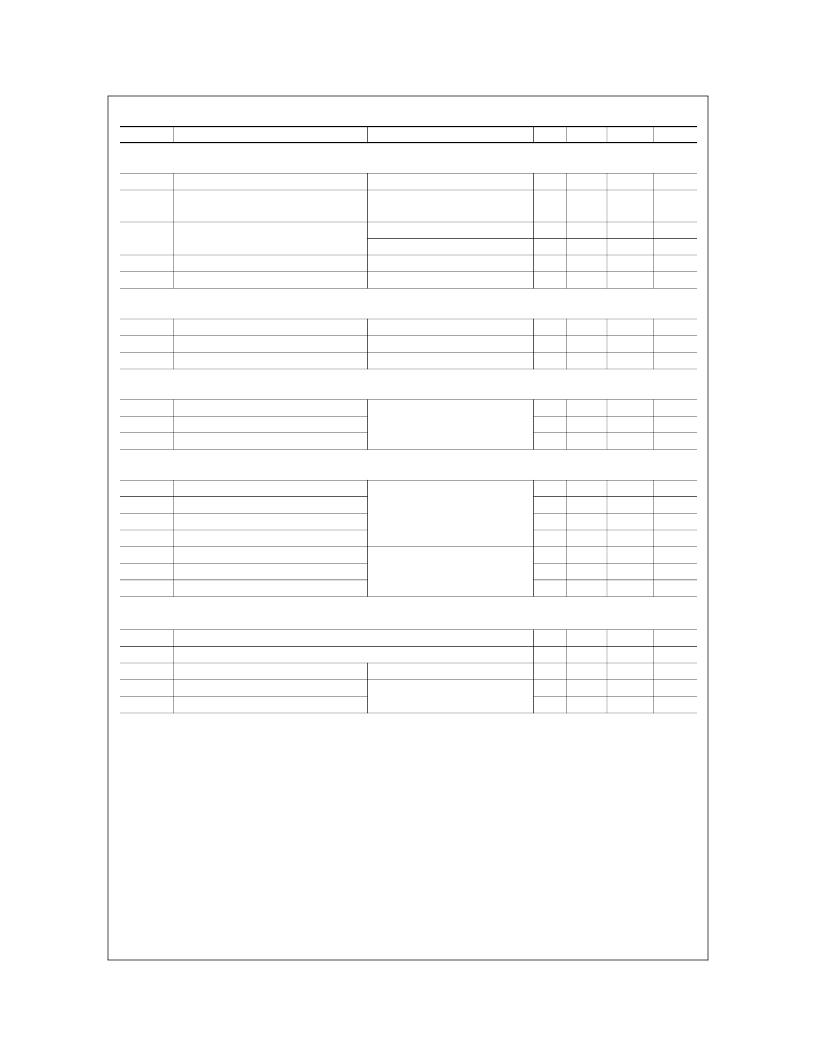
Electrical Characteristics
T C = 25°C unless otherwise noted
Symbol
Parameter
Test Conditions
Min
Typ
Max
Unit
Off Characteristics
BV DSS
? BV DSS
/ ? T J
I DSS
I GSSF
I GSSR
Drain-Source Breakdown Voltage
Breakdown Voltage Temperature
Coefficient
Zero Gate Voltage Drain Current
Gate-Body Leakage Current, Forward
Gate-Body Leakage Current, Reverse
V GS = 0 V, I D = 250 μ A
I D = 250 μ A, Referenced to
25°C
V DS = 60 V, V GS = 0 V
V DS = 48 V, T C = 150°C
V GS = 25 V, V DS = 0 V
V GS = -25 V, V DS = 0 V
60
--
--
--
--
--
--
0.06
--
--
--
--
--
--
1
10
100
-100
V
V/°C
μ A
μ A
nA
nA
On Characteristics
V GS(th)
R DS(on)
Gate Threshold Voltage
Static Drain-Source On-Resistance
V DS = V GS , I D = 250 μ A
V GS = 10 V, I D = 1.4 A
2.0
--
--
0.11
4.0
0.14
V
?
g FS
Forward Transconductance
V DS = 25 V, I D = 1.4 A
(Note 4)
--
3.0
--
S
Dynamic Characteristics
C iss
C oss
C rss
Input Capacitance
Output Capacitance
Reverse Transfer Capacitance
V DS = 25 V, V GS = 0 V,
f = 1.0 MHz
--
--
--
240
90
15
310
120
20
pF
pF
pF
Switching Characteristics
t d(on)
t r
t d(off)
t f
Q g
Q gs
Q gd
Turn-On Delay Time
Turn-On Rise Time
Turn-Off Delay Time
Turn-Off Fall Time
Total Gate Charge
Gate-Source Charge
Gate-Drain Charge
V DD = 30 V, I D = 6.5 A,
R G = 25 ?
V DS = 48 V, I D = 13 A,
V GS = 10 V
(Note 4, 5)
(Note 4, 5)
--
--
--
--
--
--
--
5
25
8
15
5.8
2.0
2.5
20
60
25
40
7.5
--
--
ns
ns
ns
ns
nC
nC
nC
Drain-Source Diode Characteristics and Maximum Ratings
I S
I SM
Maximum Continuous Drain-Source Diode Forward Current
Maximum Pulsed Drain-Source Diode Forward Current
--
--
--
--
2.8
11.2
A
A
V SD
t rr
Drain-Source Diode Forward Voltage
Reverse Recovery Time
V GS = 0 V, I S = 2.8 A
V GS = 0 V, I S = 13 A,
--
--
--
39
1.5
--
V
ns
Q rr
Reverse Recovery Charge
dI F / dt = 100 A/ μ s
(Note 4)
--
40
--
nC
Notes:
1. Repetitive Rating : Pulse width limited by maximum junction temperature
2. L = 12.6mH, I AS = 2.8A, V DD = 25V, R G = 25 ?, Starting T J = 25°C
3. I SD ≤ 13A, di/dt ≤ 300A/us, V DD ≤ BV DSS, Starting T J = 25°C
4. Pulse Test : Pulse width ≤ 300 μ s, Duty cycle ≤ 2%
5. Essentially independent of operating temperature
?20 0 2 Fairchild Semiconductor Corporation
FQ T13N06 Rev. C0
www.fairchildsemi.com
发布紧急采购,3分钟左右您将得到回复。
相关PDF资料
FQT1N60CTF_WS
MOSFET N-CH 600V 200MA SOT-223-4
FQT3P20TF_SB82100
MOSFET P-CH 200V 670MA SOT-223-4
FQT4N20LTF
MOSFET N-CH 200V 0.85A SOT-223
FQT4N25TF
MOSFET N-CH 250V 0.83A SOT-223
FQT5P10TF
MOSFET P-CH 100V 1A SOT-223
FQT7N10LTF
MOSFET N-CH 100V 1.7A SOT-223
FQT7N10TF
MOSFET N-CH 100V 1.7A SOT-223
FQU10N20CTU
MOSFET N-CH 200V 7.8A IPAK
相关代理商/技术参数
FQT1N60C
制造商:FAIRCHILD 制造商全称:Fairchild Semiconductor 功能描述:N-Channel QFET MOSFET 600V, 0.2 A, 11.5 Ohm
FQT1N60CTF_WS
功能描述:MOSFET 600V 0.2A 11.5Ohm N-Channel RoHS:否 制造商:STMicroelectronics 晶体管极性:N-Channel 汲极/源极击穿电压:650 V 闸/源击穿电压:25 V 漏极连续电流:130 A 电阻汲极/源极 RDS(导通):0.014 Ohms 配置:Single 最大工作温度: 安装风格:Through Hole 封装 / 箱体:Max247 封装:Tube
FQT1N60CTF-WS
制造商:FAIRCHILD 制造商全称:Fairchild Semiconductor 功能描述:N-Channel QFET MOSFET 600V, 0.2 A, 11.5 Ohm
FQT1N80
制造商:FAIRCHILD 制造商全称:Fairchild Semiconductor 功能描述:N-Channel MOSFET
FQT1N80TF
制造商:Rochester Electronics LLC 功能描述: 制造商:Fairchild Semiconductor Corporation 功能描述:
FQT1N80TF_WS
功能描述:MOSFET 800V 0.2A 20Ohm N-Channel RoHS:否 制造商:STMicroelectronics 晶体管极性:N-Channel 汲极/源极击穿电压:650 V 闸/源击穿电压:25 V 漏极连续电流:130 A 电阻汲极/源极 RDS(导通):0.014 Ohms 配置:Single 最大工作温度: 安装风格:Through Hole 封装 / 箱体:Max247 封装:Tube
FQT1N80TFWS
制造商:FAIRCHILD 制造商全称:Fairchild Semiconductor 功能描述:N-Channel MOSFET
FQT26N03L
制造商:未知厂家 制造商全称:未知厂家 功能描述:TRANSISTOR | MOSFET | N-CHANNEL | 30V V(BR)DSS | 5.9A I(D) | SOT-223
